Intel spends more than $400 million on the first EUV High-NA machine to lead next-generation chips
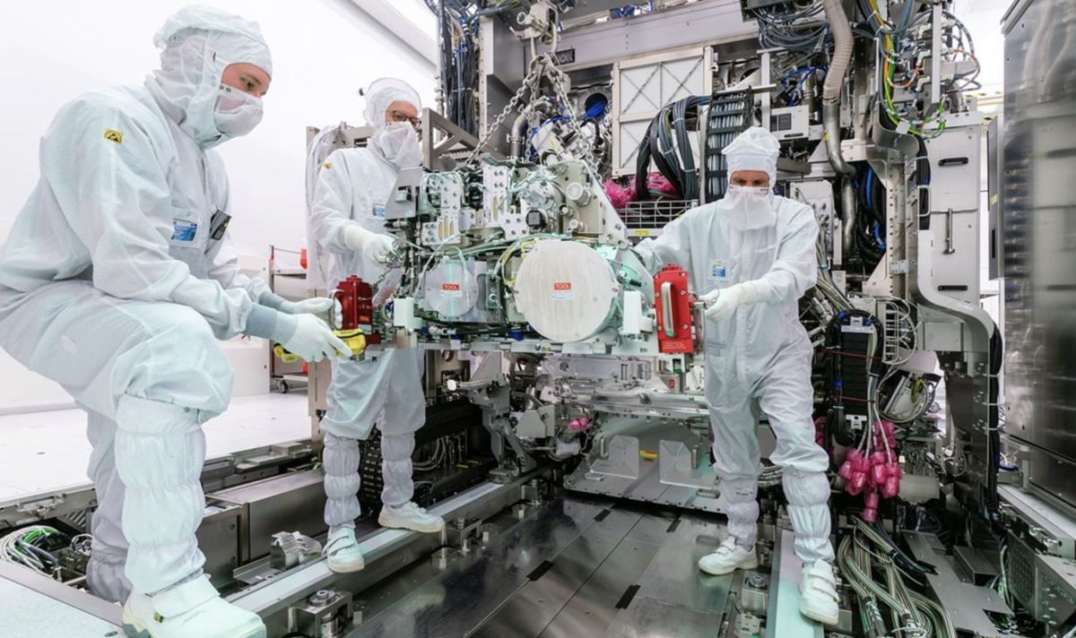
Intel today received the first high NA EUV machine after a disbursement of between 300 and 400 million dollars to lead the production of new generation chips.
A spokesperson for ASML, the company behind the development of this type of machine, explained: “We are shipping the first high NA system and announced it in a social media post today. It is going to Intel as planned and previously announced “.
This, believe it or not, marks the beginning of the development of powerful chips for computers or all types of devices and puts Intel back at the forefront, according to what they point out from Phone Arena.
The reason? It’s time to explain a little about what this type of EUV machines consist of.
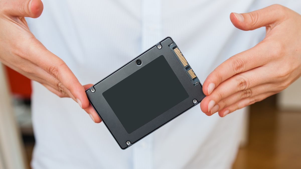
The chips feature billions of transistors, circuit patterns etched into the silicon wafer that are eventually cut into individual dies that must be ridiculously thin. And that’s where the High-NA EUV machine comes into play.
A quick explanation: the higher the NA number, the higher the resolution of the pattern etched onto the silicon wafer. While current EUV machines have an aperture of .33 (equivalent to 13nm resolution), High-NA machines have an aperture of .55 (equivalent to 8 nm resolution).
This means that with a higher resolution pattern transferred to a wafer, the foundry could avoid having to run a wafer through the EUV machine twice. to add additional features, saving time and money.
The high NA EUV machine tries to reduce the size of transistors and increase the density to pack more transistors inside a chip. The higher the transistor count on a chip, the more powerful and energy efficient it will be. With the High-NA machine, features can be made 1.7 times smaller with a 2.9 times increase in density.
To be clearer: These new machines will help bring application processor production to 2nm and below.
Currently, the Dutch company is the only one that manufactures EUV machines and the truth is that it attracts a lot of attention. They are approximately the size of a school bus and each machine has a price of 150 million dollars. Furthermore, sending it is not an easy task. It is broken down into 13 large containers and 250 boxes. Assembling the machine might be a little more complicated than putting together the bike you bought your child for the holidays.
The company expected to ship 60 EUV machines this year and, as I already told you, the first shipment is headed to Intel, which will use it for its 18A 1.8 nm process node, scheduled to begin mass production in 2025.
Beyond this, the future looks promising. Just last week, TSMC finally joined forces with samsung Foundry to address its post-2nm roadmap. Both plan to build semiconductors using a 1.4nm node in 2027. 2nm production is expected to begin in 2025, and a few days ago TSMC allowed apple to see a 2nm prototype chip.